Deep ultraviolet with short wavelength is used in many fields, such as germicidal lamp. Mercury lamp is the main light source of germicidal lamp, but led which can effectively produce deep ultraviolet without mercury is being developed. At the forefront of this field is Hideki Hirayama, director researcher of Hirayama quantum Photonics Research Office of Japan Institute of physics and chemistry.
The blue LED is followed by the UV LED
The invention of blue LED (light emitting diode), which has been considered difficult to realize for many years, has given birth to energy-saving and long-life lighting appliances and displays, and greatly changed the world. At present, one of the latest frontier research is to produce UV LED with shorter wavelength than blue LED.
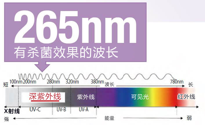
Figure 1: the visible light range of human eye is 380-780 nm. The wavelength of ultraviolet is divided into three regions: UV-A to UV-C. the wavelength range of UV-B and UV-C is called "deep ultraviolet". The absorption peak of DNA is about 265 nm deep ultraviolet, which has strong bactericidal effect. (nm: nanometer)
Among the ultraviolet rays, the deep ultraviolet ray with short wavelength has high bactericidal ability, which is expected to be used in factories and water treatment plants (Fig. 1). At present, most of the germicidal lamps use mercury. However, with the entry into force of the Minamata Treaty on mercury in 2017, the international community has begun to work to reduce the use of mercury. In this context, deep UV LED is expected. The products using deep UV LED have been on the market, but the luminous efficiency and output power are insufficient.
Hirayama, who began to study UV LED in 1996, said with confidence: "although the development competition is very fierce, the deep UV LED we developed has achieved 20.3% of the world's highest luminous efficiency. However, in order to achieve popularization, the luminous efficiency needs to be further improved, surpassing the low-pressure mercury lamp used as germicidal lamp, and the current goal is to exceed 30% ".
The basic structure of LED is the PN junction formed by the combination of n-type semiconductor with more electrons and p-type semiconductor with less electrons (with holes). After the voltage is applied, electrons and holes combine and emit light. However, the color (wavelength) of light and the voltage required for light emission are different according to the types of semiconductors. In order to develop semiconductors that can produce light of the required wavelength, a large number of researchers have explored a variety of materials. "If you can only emit light in the ultraviolet region, it's not practical," Hirayama said. Because it also needs to be more efficient than the previous light source, and can be mass produced at a lower cost. Aluminum gallium nitride (AlGaN) is expected as a promising material, but there are many problems.
New technology of generating uniform crystal
Led forms PN junction by making the crystal with ordered arrangement of atoms grow on the base material (substrate). Sapphire (Al2O3) is a cheap substrate for semiconductor. However, due to the different distances (lattice constants) between atoms, the defects called lattice defects will appear when AlGaN crystals grow. When the defect density (through dislocation density) increases, the luminous efficiency will decrease.
Blue LEDs need to form GaN crystal film with less defects on the substrate. The technology to realize this film was developed by Nagasaki Nagasaki, a lifelong professor of Nagasaki University who won the Nobel Prize. In deep UV LED, AlN crystal film is formed on the substrate and AlGaN crystal is grown on it. Hirayama has established a method to reduce defects by forming high quality AlN films on substrates. "This method made a breakthrough in improving luminous efficiency, surpassing the U.S. team of competitors," he recalled.
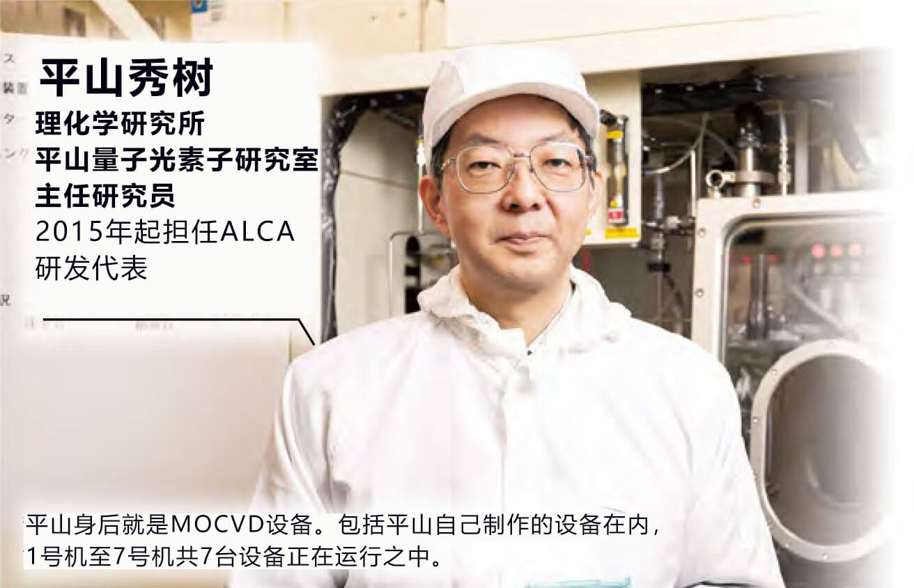
AlN crystals were fabricated by organic metal chemical vapor deposition (MOCVD). The sapphire substrate is supplied with gaseous material at about 1400 ℃ for crystal growth. The method developed by Hirayama firstly grows nitrided AlN as the core on the substrate, and then blows ammonia into the substrate in pulse shape to make it grow laterally to fill the gap between the cores. Then the gas is continuously supplied and stacked vertically. By repeating this crystal growth process, a high quality AlN layer without cracks can be formed (Fig. 2). "To make a neat crystal, you need to finely control the concentration, flow rate and reaction temperature of the gas," Hirayama said. Under high temperature, the air flow is easy to be disordered, which requires rich experience. Therefore, the equipment is semi self-made, and has been improved according to the needs. ".
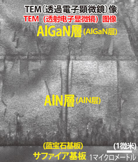
Fig. 2: it is found by TEM that the dislocation density of the crystal is higher in the initial layer of AlN layer growth, but with the further growth, the crystal becomes neat. The dislocation density of AlGaN layer is low.
Improve luminous efficiency by working on the structure
The luminous efficiency is related to three factors. The first is "internal quantum efficiency", the second is "electron injection efficiency", and the third is "light extraction efficiency". Pingshan is working hard to improve these three kinds of efficiency.
The internal quantum efficiency is the value of the ratio of electron and hole pairs generated with the current, which indicates the degree of smooth luminescence of the light-emitting layer. The internal quantum efficiency is successfully improved by making the crystal grow orderly and reducing defects.
The electron injection efficiency refers to the proportion of the injected current into the light-emitting layer. In the past, the injected electrons did not enter the light-emitting layer, but leaked from the p-layer side.
"The reason is that there is an imbalance between the number of holes in p-type semiconductors and the number of electrons in n-type semiconductors," Hirayama said. Since it is difficult to increase the number of holes, an electron barrier layer (multiple quantum barrier) is formed to reflect the electrons that are not bound but pass through directly, thus effectively combining "(Fig. 3). Thus, the electron injection efficiency is greatly improved.
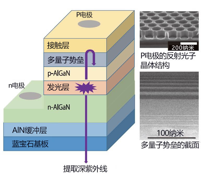
Fig. 3: in order to improve the luminous efficiency, the multi quantum barrier is used to reflect electrons, so that they are all re combined in the luminous layer. In addition, by making the contact layer transparent, the absorption of light is suppressed, and the high reflection photonic crystal is used for reflection, the light extraction efficiency is improved.
At present, the problem is how much of the light energy generated by the luminous region is extracted to the outside, that is, the light extraction efficiency. In order to avoid the generated light being absorbed inside the device structure, the method of extracting light to the outside is being studied. Pingshan said that although this is a difficult problem, it has gradually found a breakthrough.
"The main reason for the low light extraction efficiency is that the deep ultraviolet light generated is absorbed by the contact layer," Hirayama said. Therefore, absorption can be prevented by changing the path of reflection before absorption by the contact layer.
A high reflectivity photonic crystal is used in the contact layer, and a sapphire lens is installed on the light extraction side. In addition, in order to use the light scattering effect to reduce the deep ultraviolet reflection of sapphire substrate, the substrate was processed. Through these methods, the light extraction efficiency of less than 10% is increased to about 5 times. In the future, in order to peel off sapphire substrate and extract light, aluminum nitride columnar structure is planned. The simulation results show that the light extraction efficiency is expected to reach 70%.
By improving the three factors related to the luminous efficiency, it is expected to achieve the luminous efficiency higher than that of low-pressure mercury lamp.
The dream is to apply it to laser light source
The deep UV LED developed by AlGaN also has advantages in application range. "By changing the composition of the crystal, the wavelength of deep UV can be adjusted, which is also a feature. At present, deep UV LED has been realized in the band of 222-351 nm. It can freely generate deep ultraviolet light of the required wavelength according to the use, such as 310 nm light for the treatment of atopic dermatitis and psoriasis "(Fig. 4).
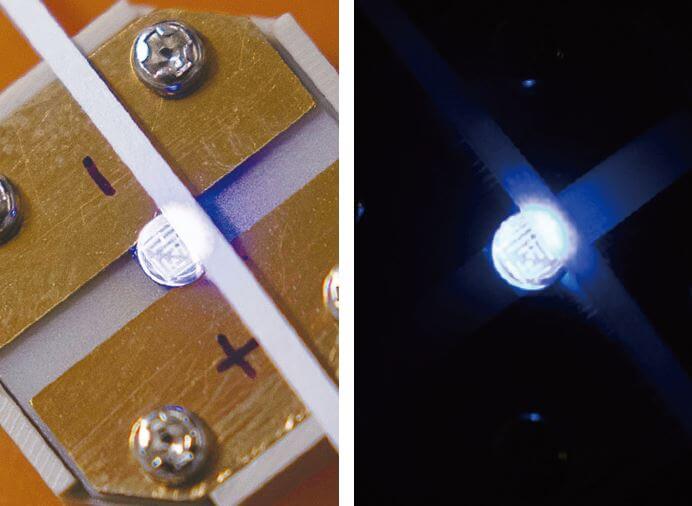
Figure 4: deep UV LED that produces 270 nm deep UV. It began to be sold for sterilization in 2014.
This is a technology in the process of development, which needs to increase the output power from tens of milliwatts to several watts. It is expected to be used in sterilization, water purification, air purification, medical treatment, biochemical industry, resin hardening and processing, printing and coating and other fields in the future.
Looking ahead, Hirayama said: "in the future, we plan to develop deep UV laser diodes (LD) with higher output power. If it can be realized, it should also be able to decompose large capacity storage media and harmful substances with capacity exceeding that of Blu ray disc.
Deep UV LED development space is still very large.
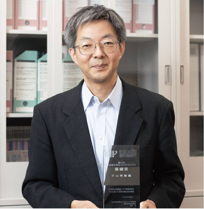
Hirayama has opened up a way for the practical application of deep UV LED. For this reason, Hirayama won the 9th semiconductor electronics Performance Award (akasaki Yong Award) and was highly praised. Hideki Hirayama is holding the Nagasaki award trophy.